In my last post Designing and Fabricating a Microwave Microstripline Filter: From HFSS Simulation to PCB Testing, I designed, simulated and manufactured a Interdigital microstrip bandpass filter for the 5.5 GHz microwave band. One common issue with microwave filters designed for a specific frequency is the presence of spurious out-of-band responses, often occurring at harmonic frequencies, particularly even multiples of the center frequency.
This becomes particularly problematic in systems involving mixers, where spurious passbands can allow higher-order mixing products or image frequencies to leak through. Mixers inherently generate sum and difference frequencies (e.g., fLO ± fIF), as well as unwanted intermodulation products at nfLO ± mfRF. If the filter passes these spurious frequencies due to poor out-of-band rejection, they can appear at the output and degrade signal purity, increase adjacent channel interference, or cause desensitization in receiver front ends. Effective suppression of these spurious bands is therefore essential to maintain mixer linearity and ensure clean frequency conversion. To address this, a low-pass filter can be cascaded immediately after the bandpass filter. This second stage effectively suppresses higher-order spurious responses that leak through the bandpass filter’s upper stopband. By cascading the two filters, the system benefits from the selective passband of the first stage and the broadband harmonic rejection of the second, resulting in a much cleaner output spectrum. Proper impedance matching between the stages is critical to avoid reflection losses and preserve the desired filter performance.
the bandpass filter
I set out to design a cascaded filter that would effectively provide good in-band characteristics and suppress higher order responses. Here was my design criteria:
- Passband center frequency of 5.5GHz
- Filter bandwidth of approximately 800 MHz
- Passband insertion loss of < 1.5 dB
- Passband ripple < 1 dB
- Suppression of out-of-band spurious frequencies > 40 dB
I also wanted to try a different design from the original post, which utilized an interdigital design of the Chebyshev type. I wanted to try a hairpin design, which are typically easier to design:
- Topology Simplicity
- Hairpin filters are just folded parallel-coupled line filters.
- Folding the λ/2 resonators into U-shapes makes them compact without changing coupling behavior significantly.
- Standard Design Flow
- Easily designed using standard Chebyshev lowpass prototype → coupling matrix → physical dimensions.
- Well-supported in design tools.
- No Grounded Resonators
- Unlike interdigital filters, which often require grounded ends (via stitching), hairpins are fully open-ended.
- This simplifies fabrication and tuning and avoids issues with via inductance.
Once again, I used HFSS to experiment with a design. I knew that for a hairpin filter, I would need half-wave resonators folded into a U shape, alternating in vertical orientation.
To design a half-wavelength resonator for a microstrip bandpass filter, we will use the guided wavelength 

where:
is the speed of light in vacuum,
is the design frequency,
is the effective dielectric constant, which accounts for both the dielectric constant of the substrate and the geometry of the microstrip line.
We’ll get into that formula more in a bit, but I want to focus on another critical part of the design, determining the proper trace width for our microstrip resonators, inductors and capacitors. Since we will ultimately be using the JLCPCB service for our prototype, I chose the following parameters for PTFE Teflon:

Let’s start with the calculation for the proper width of the 50 Ω microstrip feedline, which depends on the substrate’s dielectric constant 


Theoretical Background
The characteristic impedance of a microstrip line depends on:
- The dielectric constant
- The height
- The thickness
- The desired impedance

Hammerstad and Jensen provided empirical formulas to compute a intermediate variables 


Step-by-Step Equations
Step 1: Compute A

Step 2: Compute B

Step 3: Choose the Narrow or Wide Line Formulas
First calculate

If the result is 

![\frac{w}{h} = \frac{2}{\pi} \left[ B - 1 - \ln(2B - 1) + \frac{\varepsilon_r - 1}{2\varepsilon_r} \left( \ln(B - 1) + 0.39 - \frac{0.61}{\varepsilon_r} \right) \right]](https://s0.wp.com/latex.php?latex=%5Cfrac%7Bw%7D%7Bh%7D+%3D+%5Cfrac%7B2%7D%7B%5Cpi%7D+%5Cleft%5B+B+-+1+-+%5Cln%282B+-+1%29+%2B+%5Cfrac%7B%5Cvarepsilon_r+-+1%7D%7B2%5Cvarepsilon_r%7D+%5Cleft%28+%5Cln%28B+-+1%29+%2B+0.39+-+%5Cfrac%7B0.61%7D%7B%5Cvarepsilon_r%7D+%5Cright%29+%5Cright%5D&bg=ffffff&fg=000&s=0&c=20201002)
Step 4: Apply Thickness Correction (if 


Final width:

Worked Example for our parameters
Let’s compute the microstrip width for the following parameters from the JLCPCB table above:
- Target impedance
- Dielectric constant
- Substrate height
- Copper thickness


Step 1: Compute A

Step 2: Compute B

This value of

Since 
Step 3: Apply Thickness Correction


Guided Wavelength and Resonator Length
As mentioned previously, for resonator applications, the guided wavelength

Using 


The guided wavelength at 

Thus, a half-wavelength resonator would be:

This provides a solid initial estimate for layout.
Sidebar – modeling and optimizing the microstrip width
I wanted to use HFSS to model a microstrip from the parameters above, so I created an HFSS model and used the “Optimetrics” feature to find the optimal width for 50 Ω. This model utilized a modal wave port design and a very small section of microstrip to speed up the simulation iterations that were needed. When the optimization is setup, a sweep of microstrip widths is selected, which can be used to create a plot of impedance vs. microstrip width. Many different variations can be included, such as varying the substrate thickness, dielectric constant, etc. It might be a useful exercise to optimize 50 Ω microstrip widths for all of JLCPCB’s board options, which I may do in a future post.

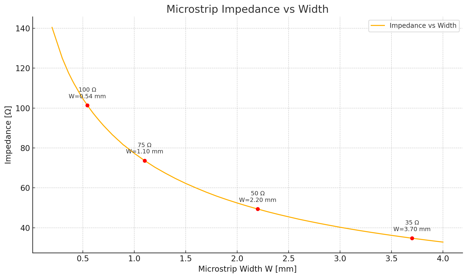
You can see that the 2.21 mm estimate from the Hammerstad and Jensen model was very close to the modeled value of 2.2 mm.
back to the bandpass filter design
I wanted a 5 pole filter in order to achieve a sharp roll off in the stop bands. I decided to create the 3D model in Ansys HFSS software using a wave port solution.

Following good RF design practices, I chamfered the folded edges of the resonators, avoiding extra material on the ends, compensating for the extra electrical length and capacitance, and keeping a more uniform impedance transition.
The calculated port impedance of the filter was very close to 50 Ω across the desired frequency range.

Next, I tried varying the spacing between adjacent resonators. What I found extremely interesting is that a uniform spacing between all of the resonators (coupling) caused a very poor response. This makes sense from my understanding of filter design, but to see the results simulated was quite striking.

In the plot above, the values in the legend indicate the spacing between the resonators in mm. Notice that the only spacing configuration that results in a flat passband is a ratio of 1:2 for the 1st and 2nd and 4th and 5th resonators (dashed lines). All other ratios result in strongly inconsistent passband insertion loss values. Also of interest is that the closer the spacing, the stronger the coupling, the lower the Q, and the larger the bandwidth of the filter design. Also, once the spacing between all of the resonators becomes large enough, the insertion loss starts to increase.
After running the simulation out to 20 GHz, it becomes apparent that there are some undesired results at equal multiples of the design frequency. Those higher-frequency responses are called spurious responses or more specifically, spurious passbands. This behavior is common in microstrip and other distributed-element filters due to their periodic structure. These spurious responses typically occur at harmonic frequencies — most often at even multiples. In my example, the response between 10 and 12 GHz is more pronounced than the next harmonic up near 15 GHz. However, these can be troublesome, especially when suppressing the image products of a mixer.

One method to mitigate this is to cascade two filters together, the first being the band pass filter followed by a low pass filter.
the low pass filter
So, I set to designing an appropriate low pass microstrip filter. There are numerous sources available containing design criteria and the filter coefficients for different low pass designs. I wanted to build a filter that utilized radial stubs as the capacitor elements.

The easiest way to design a filter like this is to model it as if it were a lumped element filter, then convert the lumped element values to microstrip components (with major caveats, as I explain below). In a distributed-element microwave filter, sections of high-impedance microstrip lines can mimic inductive behavior, while low-impedance lines can mimic capacitive behavior over a narrow frequency range. In this design, I chose the high impedance microstrip lines to have a characteristic impedance of 100 Ω , while the low impedance lines have a characteristic impedance of 25 Ω. To implement shunt capacitance more compactly, radial stubs approximately λ/4 at the design frequency can be used. These stubs act as reactive elements and help reduce layout area compared to straight-line stubs, while also offering broader bandwidth due to smoother impedance transitions.
I wrote a python program to help with the calculations, however in the book: Thomas H. Lee, Planar Microwave Engineering: A Practical Guide to Theory, Measurement, and Circuits, Cambridge University Press, in Chapter 22, the author describes lumped filter design in detail. In Chapter 23, Microstrip filters are described as being transmission line implementations of lumped filters. There is also a section specifically related to radial stub design, with approximate formulas for their design. In any case, my python code produces the following output:
python butterworth_calc.py --order 9 --fc 8500000000 --z0 50 --substrate_thickness 0.76 --copper_thickness 0.035 --trace_width 2 --high_z 100 --low_z 75 --inner_radius 0.2 --stub_angle 45 --filter_type radial --dual_stub --verbose

Filter order: 9
Cutoff frequency: 8500000000.0 Hz
Characteristic impedance: 50.0 Ω
Dielectric constant: 2.55
Substrate thickness: 0.00076 m
Copper thickness: 3.5000000000000004e-05 m
Trace width: 0.002 m
High impedance section element impedance: 100.0 Ω
Low impedance section element impedance: 75.0 Ω
Inner radius: 0.0002 m
Stub angle: 45.0 deg
High impedance section trace width: 0.5984050947383048 mm
Low impedance section trace width: 1.0883337862834337 mm

Butterworth Coefficients:
g1: 0.34729635533386066
g2: 0.9999999999999999
g3: 1.532088886237956
g4: 1.8793852415718166
g5: 2.0
g6: 1.8793852415718169
g7: 1.532088886237956
g8: 1.0000000000000007
g9: 0.34729635533386055

Stage        Value Unit
   L1 3.251408e-10    H
   C2 3.744822e-13    F
   L3 1.434350e-09    H
   C4 7.037964e-13    F
   L5 1.872411e-09    H
   C6 7.037964e-13    F
   L7 1.434350e-09    H
   C8 3.744822e-13    F
   L9 3.251408e-10    H

L1: 0.3251407745246074 μH inductor length: 0.6989376401250965 mm
L2: 1.4343501147113367 μH inductor length: 3.083345316364282 mm
L3: 1.8724110951987687 μH inductor length: 4.025021451510474 mm
L4: 1.4343501147113367 μH inductor length: 3.083345316364282 mm
L5: 0.32514077452460727 μH inductor length: 0.6989376401250963 mm
C1: 0.3744822190397537 pF stub radius for each stub pair: 2.7161111281293087 mm
C2: 0.7037963556943775 pF stub radius for each stub pair: 3.7586676634800127 mm
C3: 0.7037963556943776 pF stub radius for each stub pair: 3.758667663480013 mm
C4: 0.374482219039754 pF stub radius for each stub pair: 2.7161111281293095 mm
Notice that the Butterworth normalized coefficients are the values that can be found in any filter design handbook. The following algorithm computes the inductor and capacitor values for an n-th order Butterworth low-pass filter, given a cutoff frequency fc and a system impedance Z0.
Steps for calculating the inductor and capacitor values
- Calculate the normalized prototype element values gk for k=1,…,n using:
- Scale the prototype values to real-world component values for the given fc and Z0.
- For inductors (odd elements, g1,g3,g5,…):
- For capacitors (even elements, g2,g4,g6,…):
- For inductors (odd elements, g1,g3,g5,…):
- Output two lists: one containing the inductor values Lk, and one containing the capacitor values Ck.


Notes:
- n = filter order
- fc = cutoff frequency (Hz)
- Z0 = system impedance (Ohms)
- gk = normalized prototype coefficients from Butterworth low-pass prototype
- Inductor and capacitor values alternate in the filter.
The next step is to calculate the inductor lengths and radial stub capacitor radii. To calculate the length of an inductor, given it’s impedance Z0 (100Ω), we have to first calculate the microstrip width to achieve that impedance, then calculate the length to achieve the inductance.
Steps for calculating the Microstrip Width from Impedance
We’ll use the The Hammerstad and Jensen model again to calculate the proper width of the inductor and capacitor elements for a given impedance.
Step 1: Determine whether to use A or B
For narrow microstrip lines (


For wide microstrip lines (

![\displaystyle \frac{W}{h} = \frac{2}{\pi} \left[ B - 1 - \ln(2B-1) + \frac{\varepsilon_r - 1}{2\varepsilon_r} \left( \ln(B-1) + 0.39 - \frac{0.61}{\varepsilon_r} \right) \right]](https://s0.wp.com/latex.php?latex=%5Cdisplaystyle+%5Cfrac%7BW%7D%7Bh%7D+%3D+%5Cfrac%7B2%7D%7B%5Cpi%7D+%5Cleft%5B+B+-+1+-+%5Cln%282B-1%29+%2B+%5Cfrac%7B%5Cvarepsilon_r+-+1%7D%7B2%5Cvarepsilon_r%7D+%5Cleft%28+%5Cln%28B-1%29+%2B+0.39+-+%5Cfrac%7B0.61%7D%7B%5Cvarepsilon_r%7D+%5Cright%29+%5Cright%5D+&bg=ffffff&fg=000&s=0&c=20201002)
notes:
= Dielectric Constant
- h = Substrate height
- Z0 = system impedance (Ohms)
Step 2: Calculate Width W
Check whether to use A or B from above
if 
W = 
if
W =
Now calculate the length of the microstrip for a desired inductance
Step 1: Compute Effective Permittivity
If 

If 

Step 2: Calculate Microstrip Length

notes:
is the speed of light.
- L is the inductance in H
now we can caluculate the radii of the radial stub given the capacitance
The approximation of capacitance from a radial stub is given by:

notes:


This equation assumes quasi-static, radial field behavior between curved “plates.” It works well for rough estimation, but in practice it tends to deviate significantly from the actual capacitance observed in full-wave EM simulation.
What’s Missing in the Analytical Formula?
The formula assumes:
- A fully confined electric field within a dielectric of constant
- No field leakage into air
- Ideal transitions from feed to stub
However, real microstrip radial stubs have:
- Significant fringing fields in air, reducing effective permittivity
- Finite width feeds and metallization
- Non-uniform field distributions near the junction and edges
- Resonant and distributed effects above a few GHz
All of these cause the real capacitance to be lower than predicted.
For example, a stub with:


gives an analytical estimate:

But simulation of the actual microstrip geometry returns:

Why the Gap?
This difference arises because the simple model:
- Treats the stub like a lumped capacitor
- Ignores 3D wave propagation and fringing
- Assumes perfect field confinement
Use the analytical formula for initial sizing, but always verify radial stub performance with full-wave EM simulation. For better accuracy, tune 
I created a simulation in HFSS to calculate the capacitance of a radial stub to demonstrate the differences between the analytical and simulated values.

After running the simulation, I created a plot of the Y parameters to extract lumped-element values from the full-wave simulation data. It is possible to estimate the capacitance of a structure using the imaginary part of the input admittance, 
For a perfect capacitor, the input admittance is:

Thus, the imaginary part of the input admittance is:

Solving for capacitance:

Where:
is the resulting capacitance in farads.
is the frequency in hertz

The first thing to notice about the plot is that large inflection and reversal of the capacitance values near 7.5 GHz. This is the behavior of a distributed microstrip element, notably:
- The “reversal” in the plot shows the transition from capacitive to inductive behavior.
- It marks the resonant frequency of the stub, beyond which the lumped capacitor model fails.
- At these frequencies, the stub acts more like a resonant element or quarter-wave transformer than a simple capacitor.
Low-Frequency Behavior
At low frequencies (typically below 1 GHz), the radial stub acts as a lumped capacitor. The imaginary part of 

This results in a relatively flat, positive capacitance curve (average of 0.547 pF below 1 GHz):
- The stub stores energy in the electric field and behaves like a low-pass filter.

Mid- to High-Frequency Behavior
As frequency increases, the stub begins to support standing waves and distributed effects. This leads to resonant behavior and a transition away from ideal capacitive behavior.
At some frequency, the imaginary part of

But negative capacitance is not physical. This actually signals a transition to inductive behavior:
- The radial stub now behaves like an inductor:

This point corresponds to the resonance frequency of the stub — often near a quarter-wavelength.

So this presents a problem: designing a low pass filter for a microwave – microstrip distributed element filter using a lumped element model can be extremely problematic when the size of the elements approaches 1/4 wavelength of the signal. Notice in the plot above, that above 1 GHz and approaching the resonance frequency, the capacitance values increase exponentially.
So, going back to the original Butterworth filter problem, we would like to see a capacitance value of 0.374 pF for the first capacitor value. Let’s modify the simulation parameters to try to match that value from 0 to 6 GHz (beyond the passband of the bandpass filter).
After simulating different stub lengths, I settled on a radial stub 3.6 mm in length with a 45 deg sweep angle.

Notice that the capacitance curve is much flatter over the frequency range, which is due to the shorter stub length and thus higher resonant frequency. So what happens if we widen the sweep angle and shorten the stub further?

The average capacitance from 0-6 GHz is approximately 0.371 pF, which is very close to the 0.374 pF value we desired. Notice that the curve over the frequency range is becoming flatter, again due to the higher resonant frequency. So how could we improve this further? One method is to use two stunt radial stubs in parallel, a butterfly configuration.

In this case, I modeled the dual stubs connected to a 50 Ω transmission line. I also de-embedded the port to the stub positions to get accurate calculations of the Y-parameters. Each stub was 1.8 mm in length with a 90 degree sweep angle.


The simulated capacitance from 0-6 GHz was 0.366 pF, which is close to the desired 0.374 pF with stub lengths that are 1/2 the size of the original single stub calculation. As a result, this pushed the resonant frequency above 20 GHz as seen on the second plot above. This helped to “flatten the curve” from 0-6 GHz. Speaking of the resonant frequency of radial stub, the 1/4 resonance is calculated from the single stub length, not the combination of the stub lengths, as in the case of the admittance calculation. The first resonance typically occurs when the stub is approximately a quarter-wavelength long.

where:
is the resonance frequency in Hz
is the speed of light
is the effective length of the stub in meters
Effective Length in Radial Geometry
In a radial geometry, the electrical length depends on more than just the radius. A correction factor 

where:
is the physical radius of the stub

Example calculation for our 1.8 mm radial stub
For a stub with:


We compute:

This value corresponds well with the second plot above.

I should point out that the 1.8 mm length of the dual stubs is substantially smaller than the estimated calculation from my program when I increased the stub sweep angle to 90 degrees.
python butterworth_calc.py --order 9 --fc 8500000000 --z0 50 --substrate_thickness 0.76 --copper_thickness 0.035 --trace_width 2 --high_z 100 --low_z 75 --inner_radius 0.2 --stub_angle 90 --filter_type radial --verbose --dual_stub
Filter order: 9
Cutoff frequency: 8500000000.0 Hz
Characteristic impedance: 50.0 Ω
Dielectric constant: 2.55
Substrate thickness: 0.00076 m
Copper thickness: 3.5000000000000004e-05 m
Trace width: 0.002 m
High impedance section element impedance: 100.0 Ω
Low impedance section element impedance: 75.0 Ω
Inner radius: 0.0002 m
Stub angle: 90.0 deg
High impedance section trace width: 0.5984050947383048 mm
Low impedance section trace width: 1.0883337862834337 mm
g1: 0.34729635533386066
g2: 0.9999999999999999
g3: 1.532088886237956
g4: 1.8793852415718166
g5: 2.0
g6: 1.8793852415718169
g7: 1.532088886237956
g8: 1.0000000000000007
g9: 0.34729635533386055
Stage        Value Unit
   L1 3.251408e-10    H
   C2 3.744822e-13    F
   L3 1.434350e-09    H
   C4 7.037964e-13    F
   L5 1.872411e-09    H
   C6 7.037964e-13    F
   L7 1.434350e-09    H
   C8 3.744822e-13    F
   L9 3.251408e-10    H
L1: 0.3251407745246074 μH inductor length: 0.6989376401250965 mm
L2: 1.4343501147113367 μH inductor length: 3.083345316364282 mm
L3: 1.8724110951987687 μH inductor length: 4.025021451510474 mm
L4: 1.4343501147113367 μH inductor length: 3.083345316364282 mm
L5: 0.32514077452460727 μH inductor length: 0.6989376401250963 mm
C1: 0.3744822190397537 pF stub radius for each stub pair: 2.5994436111635832 mm
C2: 0.7037963556943775 pF stub radius for each stub pair: 3.63415913503521 mm
C3: 0.7037963556943776 pF stub radius for each stub pair: 3.63415913503521 mm
The estimated stub length is 2.6 mm compared to the 1.8 mm simulated values, a difference of 0.8 mm. A low pass filter would probably work given the estimated values, as I will show, but refining the design through simulation would produce better performance.
My first cut at the low pass filter using the estimated design parameters created a filter that seemed to make the cut for what I was looking for. I was also in a rush to combine the bandpass filter and the low pass filter for a simulation and subsequent prototype production that I decided to move ahead with what I had.


Notice that the -3 dB cutoff in the prototype design (8.5 GHz) is much higher than the simulated design (7.55 GHz). This likely due to the straight use of the prototype values. There’s also some strange behavior above 12 GHz, which could be due to the resonance of the first stub pair at approximately 13-14 GHz. In any case, the filter seems to perform well enough for my purposes in the integrated design.
sidebar – simulation of the low pass filter using optimized values
Since I proceeded with using the non-optimized values (straight from the python calculator), after completing the filter and testing it, I decided to go back and design the filter using optimized values for the inductors and capacitors.
I decided to use a radial stub sweep angle of 90 degrees to minimize the radius and thus keep the resonant frequency much higher than the desired cutoff frequency. I then calculated the lengths of the radials for the desired capacitance within a 0-8 GHz window using the radial stub model in HFSS. The average capacitances from 0 to 8 GHz in picofarads (pF) for the stubs calculated from the Y parameters:
- 1.8 mm stub (90° sweep): 0.369 pF
- 2.8 mm stub (90° sweep): 0.751 pF
This is close to the desired values:
- C1: 0.374 pF
- C1: 0.704 pF


Notice that the resonant frequency for the 1.8 mm radial stub pair is approximately 21 GHz and the 2.8 mm pair is approximately 17 GHz, both well above the desired passband cutoff.
For the microstrip inductors, I used another HFSS model.


The port was de-embedded for the calculation of the Y parameters and inductance then calculated using the following formula, assuming the network behaves like a series inductor:

Where:
is the input admittance (in siemens)
is the angular frequency (radians/second)
is the inductance (in henries)
Taking the imaginary part:

Solving for

This formula assumes that the admittance is dominated by a series inductor (i.e., the circuit behaves inductively at that frequency). The calculated values are:
- 0.9 mm inductor (0-8 GHz average): 0.362 nH
- 3.5 mm inductor (0-8 GHz average): 1.491 nH
- 4.5 mm inductor (0-8 GHz average): 2.000 nH
These match closely to the desired values:
- L1: 0.325 nH
- L2: 1.434 nH
- L3: 1.87 nH


Notice in the plots that the inductance increases rapidly when the resonant frequency is approached, so there’s a game to play of keeping the dimensions of the inductors within parameters while preventing the resonant frequency from being too low. A higher impedance trace (perhaps 125Ω vs 100Ω) would be narrower and shorter (higher resonant frequency) for a given inductance, but imposes construction challenges, i.e. overlapping radial stubs.
Putting everything together in a low pass filter design:


Notice the wider, but shorter radial stubs for the “optimized” filter compared to the original design. However, the results were surprising.

The original design performed better than the “optimized” filter, including a more gradual S21 drop off and higher S11 values, despite the component values being carefully optimized. This alone proves the need for proper modeling and simulation to achieve the optimal results.
I also wanted to see how a rectangular stub filter would compare, so I calculated the values and constructed an additional model.


Running the simulation and comparing all three filters s21:

Notice that the original design provides the best performance to suppress the spurious passband response from the original hairpin band pass filter.
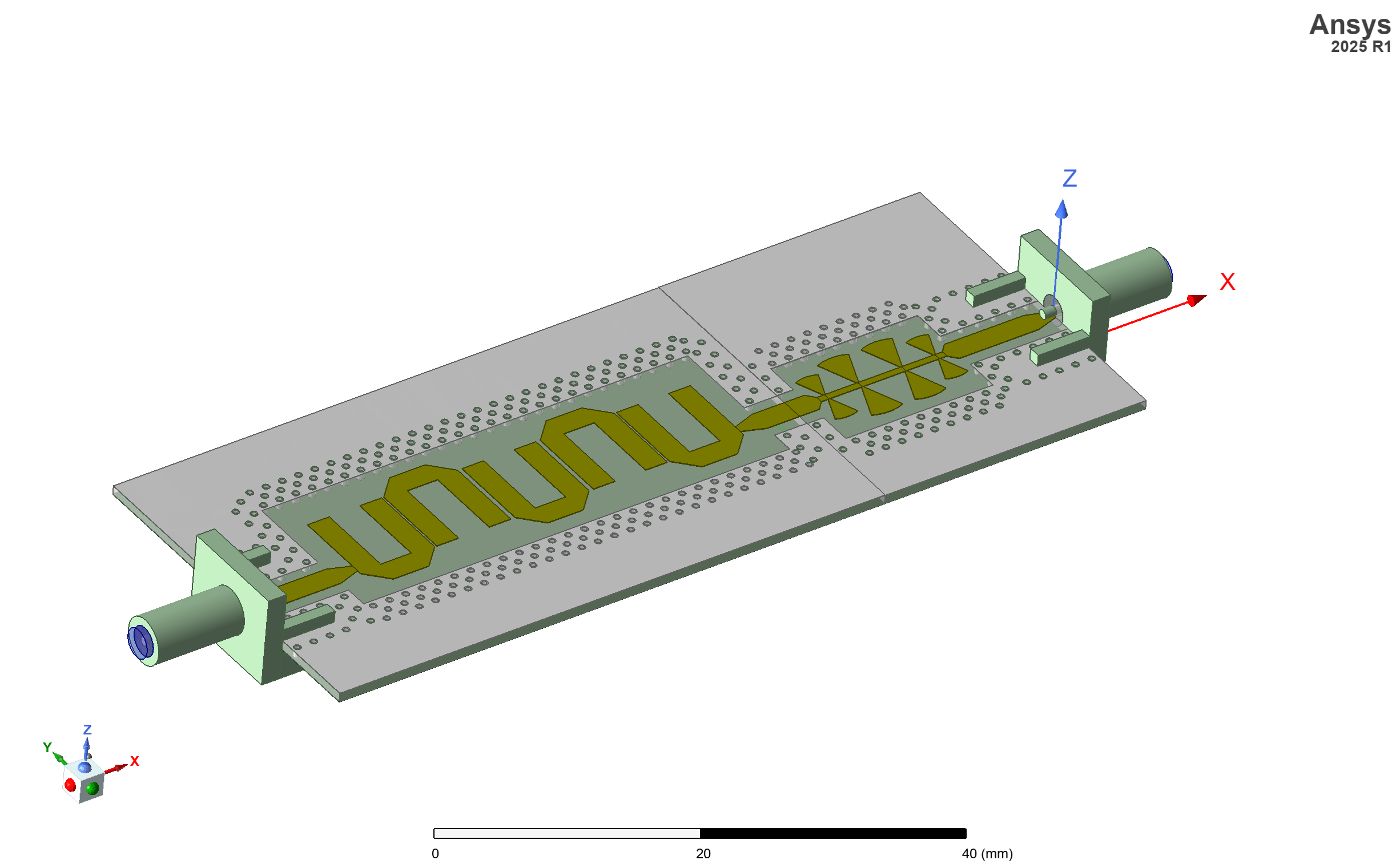
The integrated filter

For the integrated filter, I combined the bandpass filter the low pass filter components in an integrated design in HFSS. I also included an upper layer ground plane and plenty of via stitching between the ground planes.


From the plot comparison, it is clear that the spurious passband from the hairpin filter at 10-12 GHz is sufficiently suppressed with the addition of the low pass filter. The S21 values average around -40 dB or below at frequencies above the passband at 5-6 GHz. There’s some attenuation in the passband (insertion loss) due to the addition of the low pass filter, but the average in the passband is approximately -1.19 dB.

From the plot, it is evident that our desired parameters are met:
- Passband center frequency of 5.5GHz
- Filter bandwidth of approximately 800 MHz
- Passband insertion loss of < 1.5 dB
- Passband ripple < 1 dB
- Suppression of out-of-band spurious frequencies > 40 dB
(on average)
In a final bit of thoroughness, I added SMA connectors to the ports for accurate simulation of the S parameters.

Plotting S21 of the version with and without SMA connectors


So there’s not much difference in the S21 parameters between the two models with and without the SMA connectors. It’s not surprising that there are some S11 differences due to the presence of the connectors. Some mismatches in impedance are likely due to the geometry and electrical characteristics of various SMA interfaces.
I also plotted the electric fields in HFSS to look for any hot spots in some of the elements that are in close proximity.


Having developed a model sufficient for building a prototype, I designed the board using KiCad.


Identically as in the previous post, I uploaded the design files to JLCPCB to have the board manufactured. About a week later, the completed boards arrived.

As I mentioned in the previous post, my test equipment is limited to a maximum frequency of 6 GHz, so I couldn’t evaluate the prototype’s response above that frequency.


I would like to rent a good VNA with a frequency range that extends up to 20 GHz for evaluating the filter’s spurious passband suppression performance. I will follow up on this post once I am able to acquire the equipment. However, with the limited performance that I can evaluate, I’m quite satisfied with the overall performance. One thing to note is that I am not using the optimal materials for this filter at microwave frequencies. The surface roughness of the copper seems high, and this can contribute to degraded performance, including unwanted losses, especially in the higher frequencies.
A note about spurious passbands in filters
In Thomas H Lee’s book Planar Microwave Engineering, Chapter 23.2.5 describes instances in which spurious passbands can be desirable. In the case of commensurate stepped-impedance filters, reentrant passbands can be used strategically. This can be especially advantageous for millimeter wave designs where the physical limitations of constructing a traditional filter is impractical at those frequencies.