Microstripline filters are essential components in RF and microwave circuits, offering a compact and efficient way to shape frequency response. In this post, we’ll walk through the complete process of designing, simulating, fabricating, and testing a microstripline filter. Starting with electromagnetic simulations in Ansys HFSS, we’ll validate the design before exporting it to KiCad for PCB layout. After fabrication, we’ll evaluate the filter’s real-world performance using S-parameter measurements. Along the way, we’ll discuss key design choices, common challenges, and practical insights to bridge the gap between simulation and reality. Whether you’re an RF engineer, PCB designer, or just curious about high-frequency circuits, this post will provide a hands-on approach to bringing a microstrip filter from concept to working hardware.
A microstripline interdigital filter is a type of bandpass filter commonly used in RF and microwave applications to selectively allow signals within a desired frequency range while attenuating signals outside of that range. It is implemented using microstrip technology, which consists of conducting traces on a dielectric substrate with a ground plane beneath it.
How It Works
An interdigital filter consists of multiple resonant elements (typically quarter-wavelength resonators) arranged in a parallel, alternating configuration. These resonators are capacitively coupled to each other and the alternating pattern provides tight coupling between adjacent resonators, resulting in a compact design with good performance characteristics.
Applications
Microstripline interdigital filters are widely used in:
- Wireless Communication Systems – To filter out unwanted signals and interference in devices like mobile phones, Wi-Fi routers, and base stations.
- Radar and Sensing Applications – For precise frequency selection in radar front-end receivers.
- Satellites and Aerospace – Due to their lightweight and compact form factor, they are well-suited for space and airborne communication systems.
- Test and Measurement Equipment – Used in spectrum analyzers, network analyzers, and other RF testing systems to isolate specific frequency bands.
Interdigital filters are particularly attractive because they offer broad bandwidth, low insertion loss, and sharp roll-off, making them ideal for high-performance RF circuits. Their design is well-suited for PCB-based fabrication, allowing for low-cost and repeatable manufacturing.
In my application, I wanted to test the feasibility of designing an implementing a microwave filter small enough to push the limits of the COTS CAD software and manufacturing capabilities of popular PCB fabrication houses.
Tools utilized
Here’s the list of tools and services that I used to design and implement the filter:
- Ansys HFSS (High-Frequency Structure Simulator) – A powerful electromagnetic simulation software used for designing and analyzing high-frequency components like microstrip filters, antennas, and waveguides. It provides full-wave 3D simulations to optimize performance before fabrication. There are a few alternatives to HFSS with lower entry costs which could be explored, but I haven’t had the chance to review them yet.
- KiCad – A free and open-source PCB design suite that allows users to create schematics, design PCB layouts, and generate manufacturing files. It is widely used in RF and microwave PCB design, offering controlled impedance routing and footprint customization.
- FreeCAD – An open-source 3D CAD software used for mechanical design, enclosure modeling, and component integration. It is useful for designing RF housings, shielded enclosures, and custom mounts for PCB-based circuits.
- JLCPCB – A popular PCB manufacturing service known for its affordability, fast turnaround, and high-quality fabrication. It supports various PCB technologies, including high-frequency materials, making it ideal for producing RF filters and other precision circuit designs.
Reference Materials
- Thomas H. Lee, Planar Microwave Engineering: A Practical Guide to Theory, Measurement, and Circuits, Cambridge University Press.
- Marki Microwave Microstrip Filter Design Tool – An online tool for designing microstrip filters, providing calculations for dimensions and performance characteristics.
Thomas Lee’s book is an excellent reference and is a comprehensive resource for RF and microwave engineers, covering both theoretical and practical aspects of high-frequency circuit design. The book delves into microwave transmission lines, impedance matching, network analysis, and passive/active circuit components, with a strong emphasis on planar structures like microstrip and coplanar waveguides. It provides in-depth discussions on filter design, amplifiers, oscillators, and mixers.
Limitations
In order to verify the performance of the filter implementation, I needed to measure the S-parameters. Currently, I have a scalar network analyzer configuration utilizing a Signal Hound BB60C Real-time Spectrum Analyzer, TG124A Tracking Generator and a Mini Circuits Directional Coupler. These instruments, in combination with the Spike software, provide scalar S21 and S11 measurements from 11 kHz to 6 GHz. As a result, I needed to design a filter with a passband below 6 GHz in order to evaluate it. Also, I do not have phase-stable SMA cables, so the performance suffered from a small amount of measurement inconsistency due to mechanical and electrical limitations.
Design
In Thomas Lee’s book, section 23.3, the author outlines the design of parallel resonant line bandpass filters, hairpin bandpass filters, and a specific design alteration – the interdigital bandpass filter. The author states “It is inconvenient that the interdigital filter requires ground connections, and on alternate ends of the resonators at that, so this filter is not widely used in microstrip form.” Understanding the fabrication challenges presented, I decided to accept that challenge and design such a filter for fabrication on a PCB.
I wanted a tool to quickly approximate the design of my filter before constructing it in HFSS for iterative simulation and analysis. I found an online tool published by Marki Microwave: https://markimicrowave.com/technical-resources/tools/microstrip-filter-design-tool/ This tool provides an approximate physical design layout of the filter given various design criteria.
However, in order to use the tool, we must consider the design constraints of the end product. Since I wanted a quick-turnaround and relatively cheap fabrication for my prototype, I chose a popular fabrication company, JLCPCB.
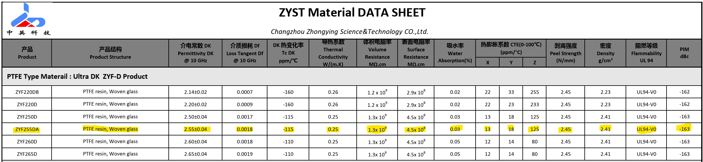
There are a few options to choose from for the board material. Since I wanted a board with as close to a controlled impedance as possible, so I chose PTFE for this prototype over Rogers due to cost considerations:

I chose the ZYF255DA material with a dielectric constant Dk=2.55 and 1 oz copper (0.035 mm thickness) with the parameters listed in the datasheet:
A Note about fr4
I would not recommend using FR4 for any RF designs. FR4 is not ideal due to its high loss tangent and inconsistent dielectric properties, which degrade signal integrity at high frequencies. Its dielectric constant (Dk) varies with frequency, leading to impedance mismatches and unpredictable performance. Additionally, FR4 has higher dissipation loss than specialized RF substrates like Rogers laminates, causing greater signal attenuation, especially at GHz and higher frequencies. For RF designs requiring low loss, precise impedance control, and minimal signal degradation, low-loss RF materials such as Rogers, or PTFE are preferred.
A listing of the design constraints for PCBs is listed at https://jlcpcb.com/capabilities/pcb-capabilities which of interest are several constraints including minimum via sizes, trace widths, trace spacing, etc.
In my past experience, I have seen that the calculated values of lumped element filters tend to produce distributed element filters with passband regions having significantly higher frequencies. Thus I intended to start the filter design with a higher-than-desired passband. I also wanted a passband that would fit within the allowable measurement parameters of my equipment, particularly in the higher end, to make the design more challenging. As a result, I chose a low frequency cutoff of approximately 5.2 GHz and an upper frequency cutoff of approximately 5.8 GHz. I then moved those frequencies up about 400 MHz to offset the design higher. Having a basic set of constraints, I plugged some parameters into the Marki Microwave filter design tool:
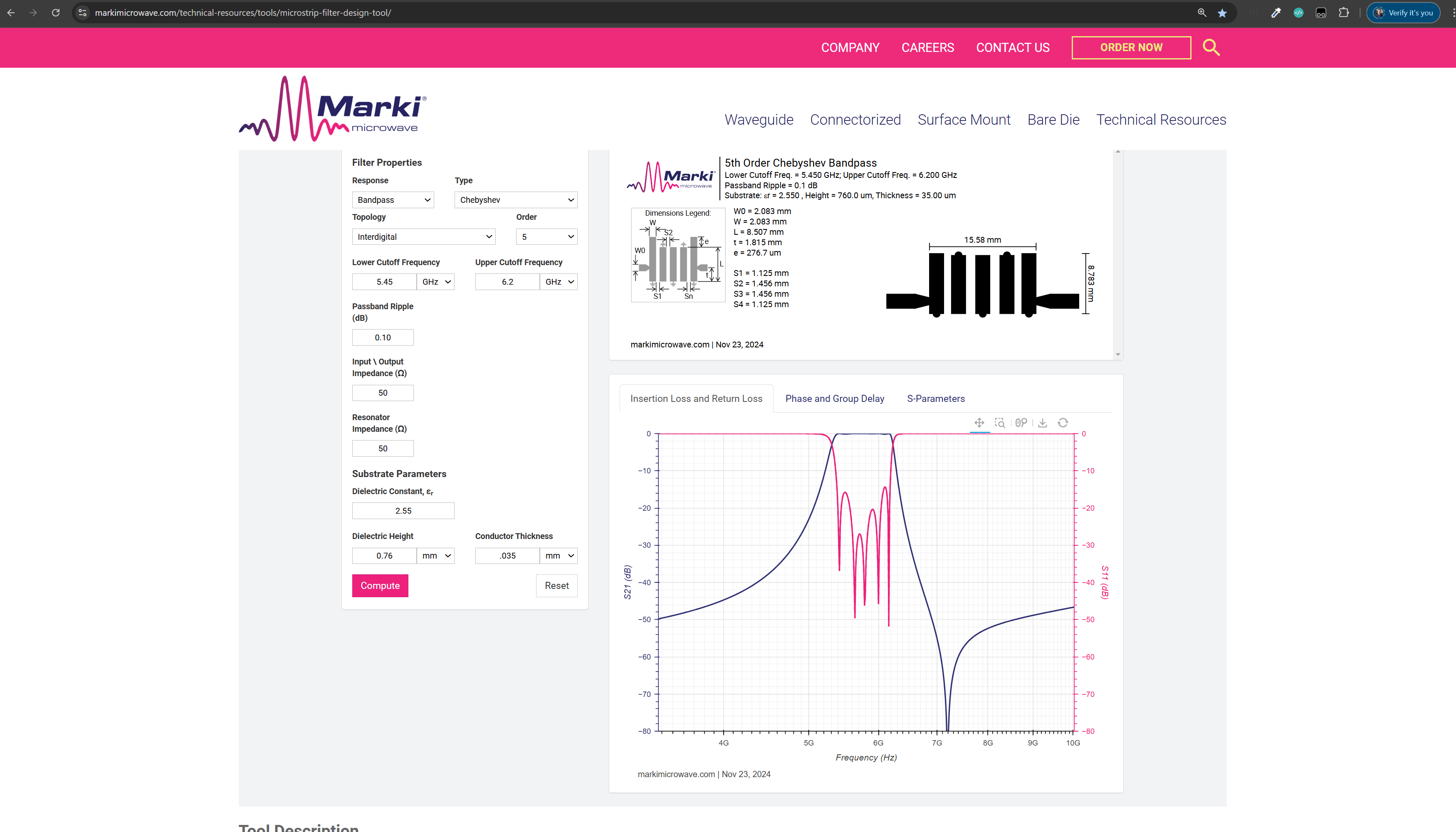
The tool provides a set of starting values for the dimensions of the microstripline elements. From there, I proceeded to construct a parametric implementation in HFSS.
Simulation
When using HFSS for simulation, parameterizing nearly every aspect of the design is crucial. The software’s intuitive interface allows engineers to replace fixed values with variables, enabling dynamic adjustments. Simply assigning a variable name prompts a dialog for value input, ensuring seamless updates across the design. This feature is highly powerful, facilitating rapid design iterations and parametric sweeps, where electrical parameters can be automatically optimized by adjusting variable values.
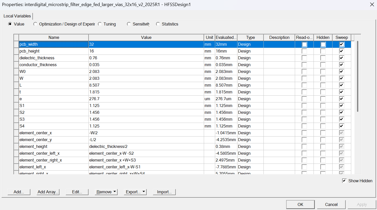
Using those parameters, I laid out the filter elements on a dual-layer PCB approximation within the HFSS modeler.
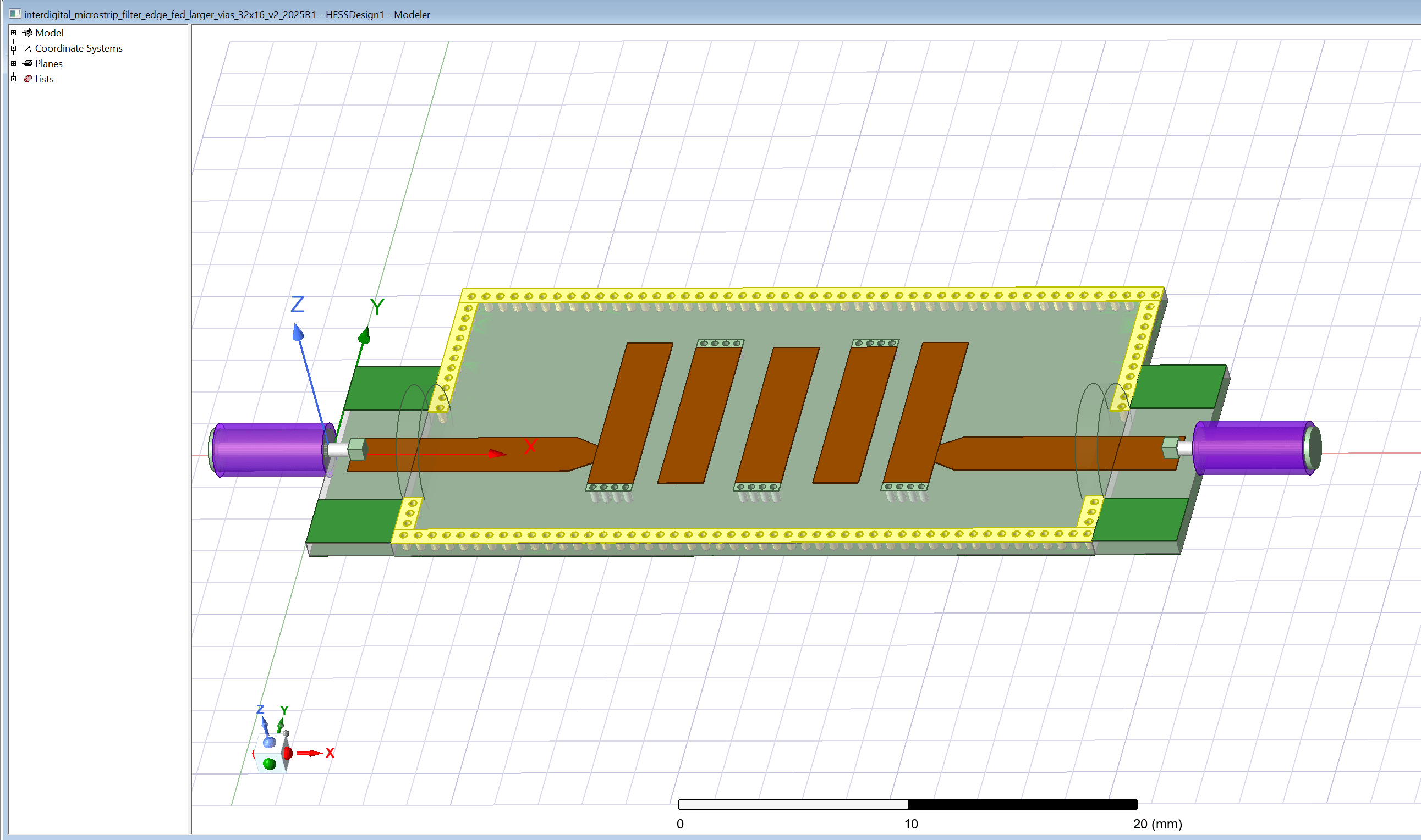
For the feed points, I wanted to model the possible impedance mismatches of coaxial SMA connectors and other unknown effects (i.e. solder joints). I decided to model a 50 ohm coaxial cable using the specifications of a specific brand of hardline coaxial cable. In HFSS, I chose a Modal solution with an auto-open region and auto-selected direct/iterative first order analysis. I also wanted to model the filter with and without a copper shield, so I included a via-stitched grounded perimeter conductor. In hindsight, I should have made the ground strip much wider to accommodate better shield attachment in the final product. The elements are also grounded on each end using via stitching.
After running the simulation and frequency sweep, the results were somewhat close to the initial approximation, with some notable differences:
- Higher insertion losses.
- Lower passband frequencies.
- More passband ripple.
- Sharper roll off in the lower passband cutoff region

to shield or not to shield
In typical integrated RF applications, most of the critical high frequency components are enclosed within grounded metallic shielding material in order to prevent EMI, minimize crosstalk and improve system performance by preventing unwanted outside signal interference. Shielding can also affect filter performance, especially in tight enclosures. Here are some of the effects:
- Affects Dielectric Properties – The presence of a metal enclosure alters the effective dielectric constant (Dk) of the microstrip substrate, which can slightly shift the filter’s center frequency and bandwidth. This shift needs to be accounted for in design simulations.
- Modifies Coupling and Impedance – In interdigital and coupled-line filters, the shield changes the electric field distribution, impacting coupling between resonators. This can affect bandwidth and insertion loss, requiring fine-tuning during the design phase.
- Introduces Cavity Resonances – If not designed properly, shielding can create unintended resonances within the enclosure, leading to spurious frequency responses that degrade filter performance. Vents, damping materials, or careful enclosure sizing help mitigate this issue.
In my application, I modeled both shielded and unshielded filters. The dimensions of the shield are set to 16x32x9 mm.
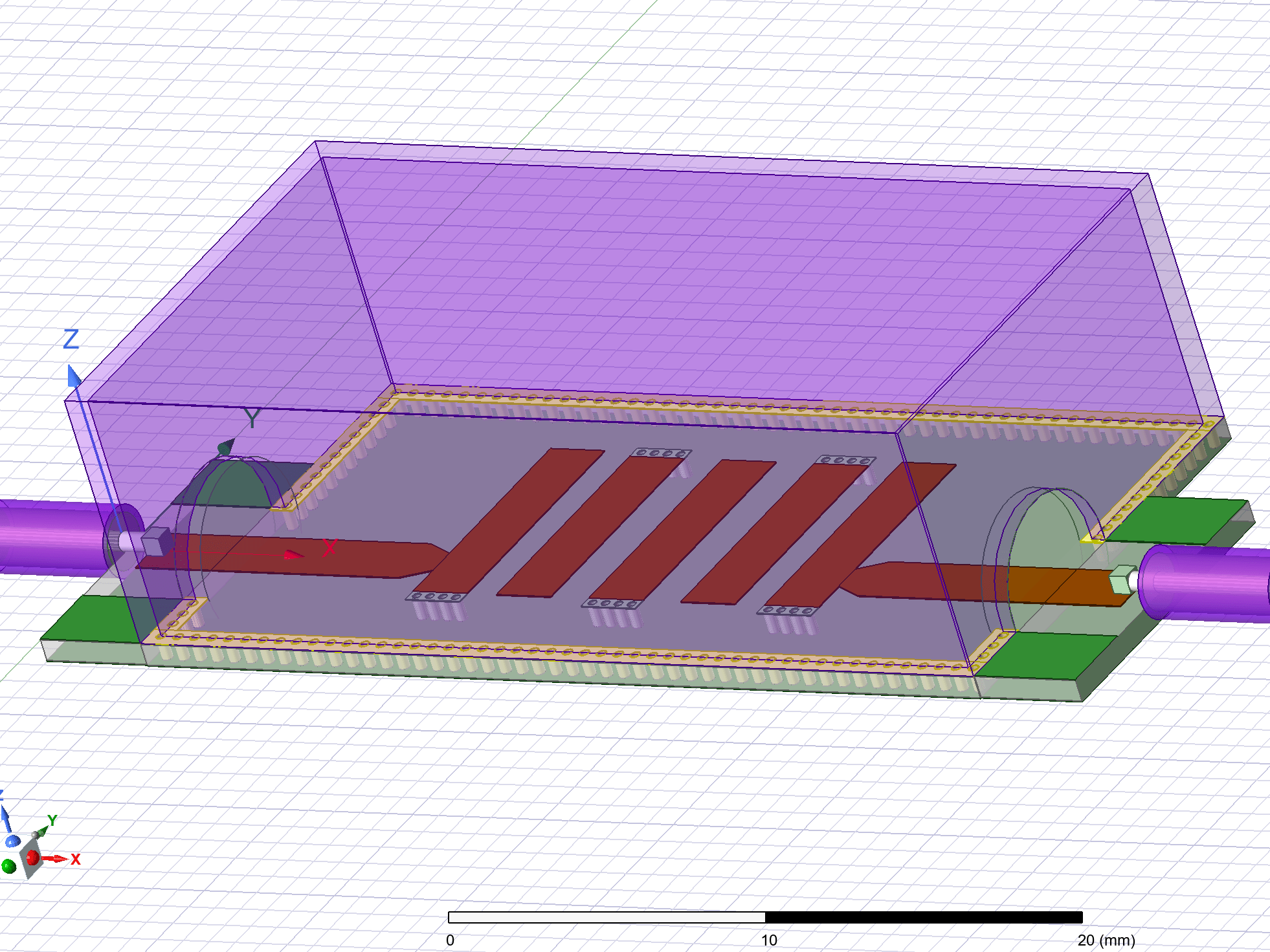

There was not much difference between the unshielded and shielded simulations other than slightly improved insertion loss and a minimally wider filter bandwidth, particularly at the lower frequency cutoff. Nonetheless, it is evident that shielding must be considered when designing the filter. When mechanical constraints dictate tight spacing and critical circuit layout, this can be critical.

I should mention that I tried several different feed configurations, but decided to concentrate on modeling the SMA edge connections as this would be the most common real-world configuration.
implementation
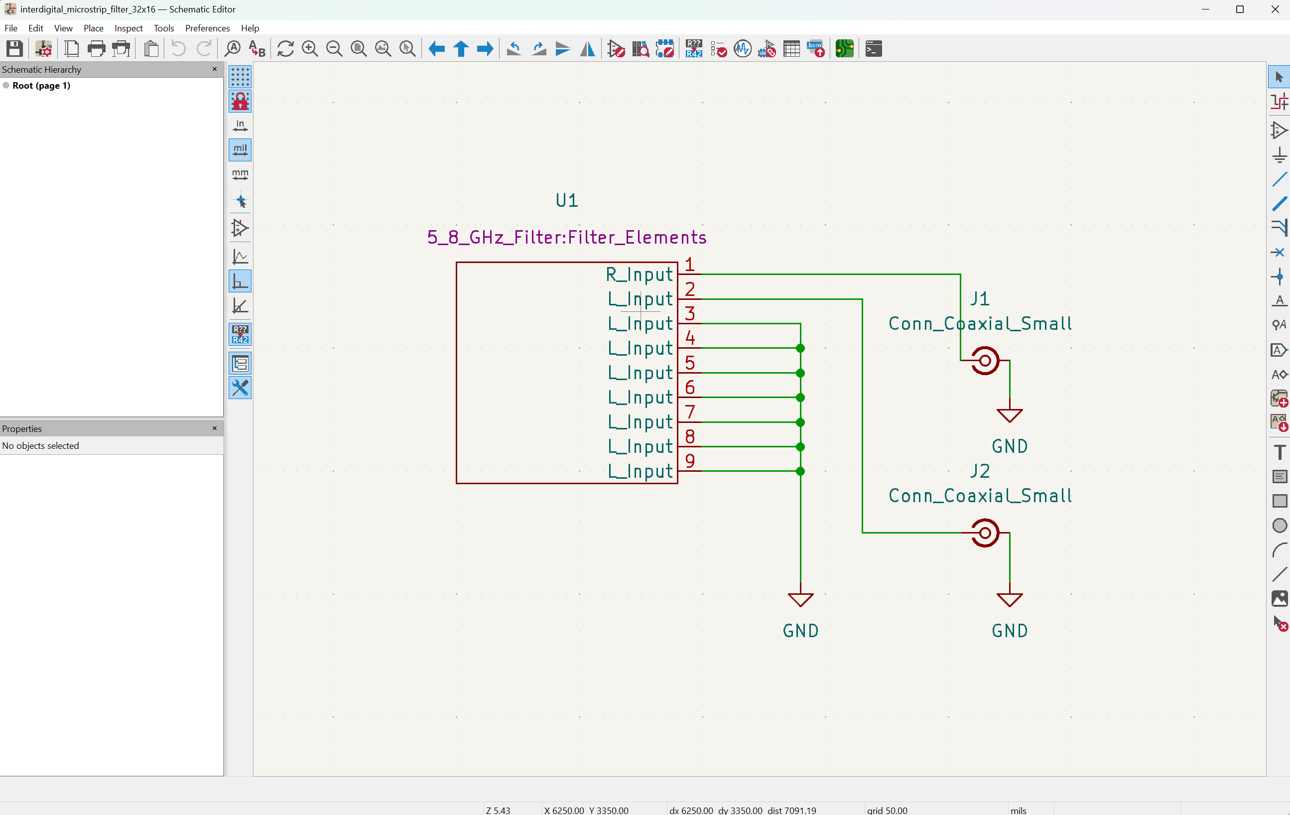
Since I was satisfied with the simulation results, the next step would be to export the model solids to an electronic design automation (EDA) suite. I chose KiCad since it is what I am most familiar with. KiCad is a powerful open-source EDA suite used for designing schematics and printed circuit boards. It provides a full workflow for PCB development, from circuit design to fabrication. KiCad is free, actively developed, and widely used by hobbyists, engineers, and professionals.
Unfortunately, I was not able to directly export the entire design from the HFSS modeler. There is no direct export function to KiCad, so I was limited to exporting AutoCad DXF files for each component. Additionally, the filter elements and shielding strips contained via stitching in the modeler that I did not want to be included in the export. KiCad has its own functionality to add vias that utilizes the constraints set by the fabrication facility. Additionally, using KiCad to create the copper layers, solder masks, silkscreens, etc. makes more sense than directly importing from HFSS.
I did run into an issue when using the DXF exports from HFSS. The vias were exported with the components, so I needed to remove them before importing them into KiCad. I also wanted to re-dimension the exports to center them properly as well as clean up any stray line segments. I used FreeCAD to import and clean the DXF files, then exported them out as DXF files for use in KiCad.
In KiCad, I decided to create my filter component as a footprint, then use that footprint in the PCB design. KiCad is a fairly complex program to learn, but is highly flexible and has integration with Python which can be very powerful when needed. Following the KiCad design workflow, I also created a schematic that utilizes the footprint, which then is implemented in the PCB editor.

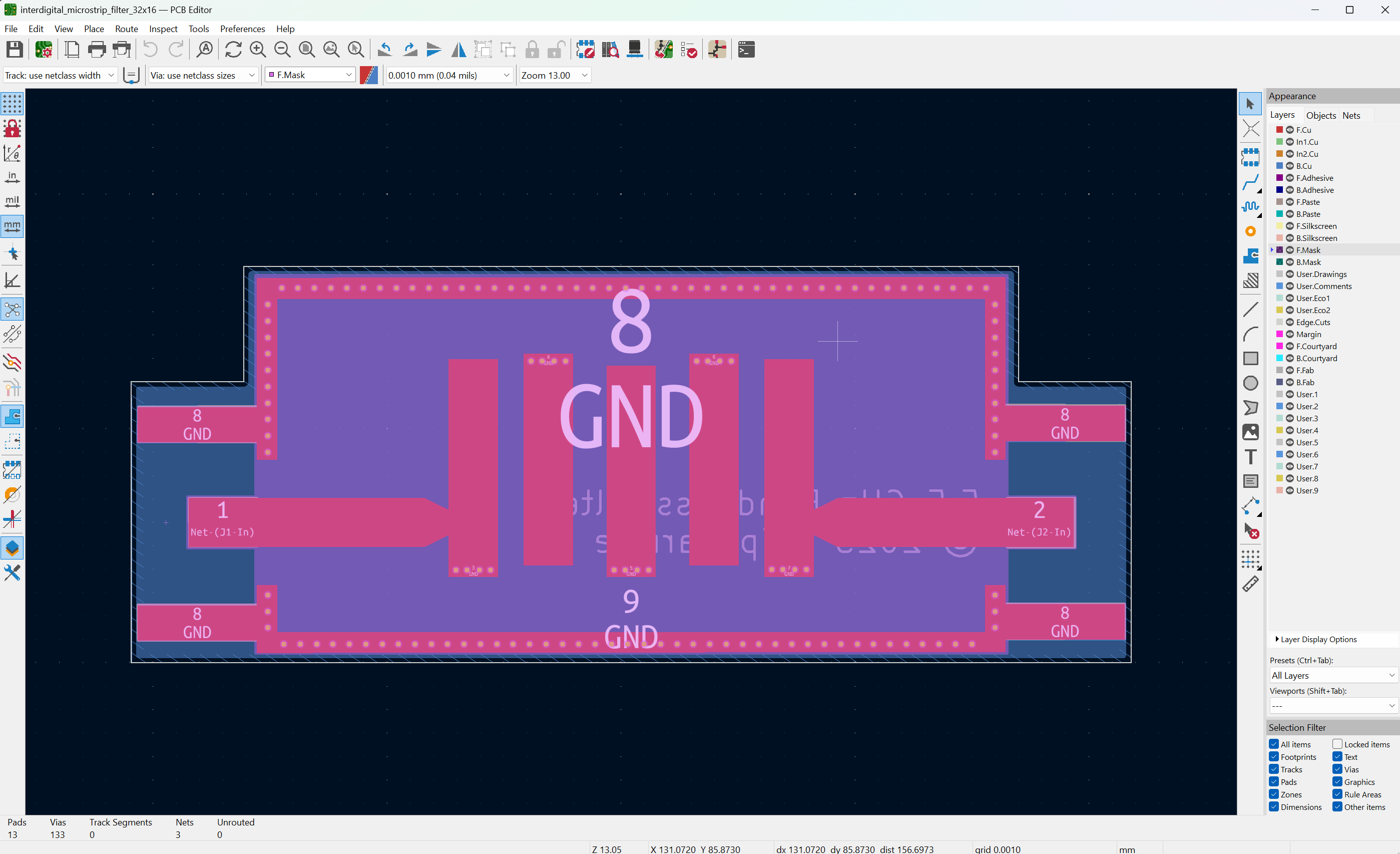

KiCAD has a design rules check (DRC) capability built in, which can be set manually or downloaded from your fabrication house of choice. I did encounter warnings after running the DRC, complaining about having a port that was shorted to ground (the filter ports and elements), but most of these can be ignored. Having completed the design in KiCad, I then created the Gerber and Drill files, exported them out of KiCad and uploaded them to JLCPCB for fabrication. JLCPCB will also run a DRC to check for consistency before sending the design to manufacturing.
After waiting one week for delivery, the completed prototype boards were delivered.


Filter PCB Front (L) and Back (R)
Testing
As mentioned previously, my testing equipment is limited to an upper frequency of 6 GHz and scalar analysis only. I have a Signal Hound BB60C Real Time Spectrum Analyzer, USB-TG124A tracking generator and a Mini Circuits ZHDC-16-63-S+ Directional Coupler https://signalhound.com/products/6-ghz-scalar-network-analyzer-w-coupler-for-rl/


When performing the analysis using the Spike software, I ran into an issue related to the mechanic/electrical stability of the cables and filter. Any time I moved the cables to attach or detach the feed through or the filter, the software calibration would become inaccurate, which would lead to measurement errors. I used high quality semi-rigid coax from Mini Circuits, but that didn’t help much. I really need to invest in a set of phase-stable cable to minimize this issue.
A Note About Phase-Stable Cables
When performing network analysis, especially at microwave and millimeter-wave frequencies, using phase-stable cables is crucial to ensure accurate and repeatable measurements. Unlike standard coaxial cables, phase-stable cables are designed to minimize phase drift due to temperature changes, mechanical movement, and flexing.
Why Phase Stability Matters
- Prevents Thermal Drift – Temperature changes can cause expansion/contraction of cable materials, leading to phase shifts that distort measurements. Phase-stable cables mitigate this effect.
- Reduces Measurement Errors – Phase variations in test cables can introduce uncertainty in S-parameter measurements, impacting calibration accuracy.
- Ensures Repeatability – Consistent phase response is essential when testing filters, antennas, and transmission lines, especially in precision applications like 5G, radar, and satellite communications.
The results of the measurements without the filter were surprisingly close to the simulation.


When I ordered the copper sheet for the shield can, the thinnest option I had was 0.5 mm copper. This posed some serious issues when cutting and bending the edges to form the shape. When I attempted to solder the shield into place, the thermal properties of the copper made it very difficult, so I applied some copper tape to cover the open edges. I should have used a thinner sheet metal other than copper. In any case, the results show that the shield did not improve the filter as much as it did in the simulation. I may try to make another filter with a different shield material and test that as well.


Of note is that the shielded version did present a steeper roll off in the lower stopband. However, the passband ripple did not improve as much as in the simulation.


The S11 measuring capabilities of my setup seem to have some limitations as evident by the ripple artifacts in the stop band. I would like to obtain a Vector Network Analyzer (VNA) with measurement capabilities well into the 10’s of GHz region in order to explore more aspects of the filter and to evaluate future designs.
In any case, I believe one could conclude from this exercise that with the correct design tools and manufacturing capabilities, high performance RF filters with excellent accuracy can be realized by the RF engineer with reasonable effort.